WSe2/hBN/MoS2 Heterostructures Reduce Scattering Effects in Semiconductor
- Details
- Category: tungsten‘s News
- Published on Saturday, 02 October 2021 23:02
Researchers at Korean University recently introduced a strategy to use remotely adjusted two-dimensional WSe2/hBN/MoS2 heterostructures doped transistors to help reduce the intrinsic scattering effects of semiconductor materials. When manufacturing electronic devices based on traditional semiconductor materials, engineers need to complete a key step, that is, doping.
Doping mainly refers to the introduction of impurities into the semiconductor to realize the control of its optical, electrical and structural characteristics. Although doping is a key step in the development of semiconductor-based electronic products, many traditional doping strategies have introduced too many carriers, leaving ionized dopants in the channel and hindering the transport of charge carriers. Therefore, some engineers have been trying to design modulation doping technology to separate ionized dopants from the channel.

The transport of charge carriers in two-dimensional semiconductors, such as transition metal dichalcogenides (TMDCs), can be affected by a number of internal and external factors. In fact, in these materials, the carriers are highly confined and are affected by the scattering effect caused by environmental factors.
Due to this susceptibility to scattering effects, so far, two-dimensional materials have proven to be very difficult to study, and researchers have not fully understood their basic physical properties. In order to study these materials, especially to study the quantum phenomena that occur within them, researchers should first eliminate unwanted scattering effects.
Eliminating scattering effects can also improve the performance of two-dimensional semiconductor-based devices, because past studies have found that these effects have an adverse effect on the performance of the devices and limit their potential for real-world applications. Although researchers have proposed several strategies to eliminate external scattering sources, so far, reducing the intrinsic scattering that occurs in two-dimensional materials has proven to be highly challenging.
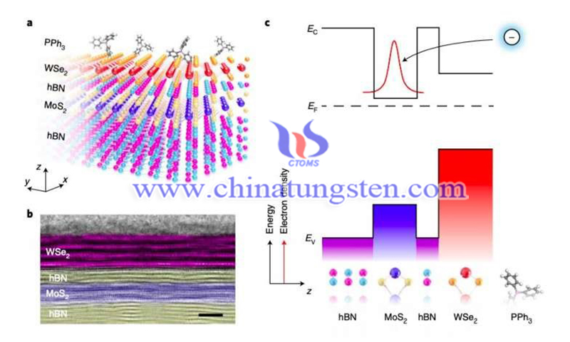
Researchers from Korean universities and other institutions in South Korea introduced a strategy that can help reduce the intrinsic scattering effects of two-dimensional semiconductor materials. This strategy was introduced in a paper published in Nature Electronics, enables the modulation of doping in 2D semiconductors through van der Waals (vdW) band engineering and remote charge transfer doping.

"Our research reports the remote modulation doping of a two-dimensional transistor composed of strip-modulated WSe2/hBN/MoS2 heterostructures," the researchers wrote in their paper. "The bottom molybdenum disulfide channel is remotely doped through the controlled charge transfer of the dopant on the tungsten diselenide surface.
Using their doping modulation strategy, the researchers were able to realize a transistor that exhibited reduced intrinsic scattering. This greatly improves the carrier mobility of the device (that is, the speed at which charge carriers move in the device).
In the future, the research conducted by this research group can pave the way for the development of faster and more efficient semiconductor-based electronic products. In fact, engineers can use the methods proposed in recent papers to control the carrier mobility and density of two-dimensional field effect transistors.
- Next >
Link to this article:WSe2/hBN/MoS2 Heterostructures Reduce Scattering Effects in Semiconductor
Reprint Statement: If there are no special instructions, all articles on this site are original. Please indicate the source for reprinting:Tungusten,Thanks!^^

