New Approach Yields High-Performance Flextronics Based on Molybdenum Disulfide
- Details
- Category: tungsten‘s News
- Published on Monday, 09 August 2021 20:59
Now, researchers at Stanford University have thought of a manufacturing method that can produce high-performance flextronics which is based on molybdenum disulfide (MoS2).
Flextronics – meaning flexible electronic products that include active and passive devices and their carriers (similar to PCBs) – is an attractive and popular area of interest, especially in wearable devices and even some IoT applications. However, it is a challenge to develop carriers and components with excellent flexibility, and robustness, and sufficient electronic performance.
So far, the main engineering obstacle is to have such devices that are so thin that it is almost impossible: the heat required to form such a flexible plastic substrate is higher than the substrate's ability to withstand it. During the production process, these flexible materials will melt and decompose at this temperature.
Now, researchers at Stanford University have thought of a manufacturing method that can produce atomically thin transistors with a length of fewer than 100 nanometers – several times smaller than those made by traditional methods. Their solution looks a bit anomalous: They perform the process in a series of steps, starting with a rigid silicon substrate coated with glass.

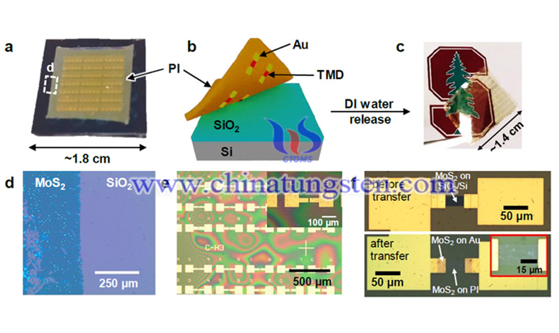
The transfer process for 2D monolayers with contacts: (a) Optical image of MoS2and patterned metal covered by polyimide (PI) on SiO2/Si. (b) Schematic of the transfer process: the PI with embedded metal contacts and monolayer transition metal dichalcogenides (TMDs) are released from the rigid growth substrate. (c) Optical image of the flexible PI after transfer. Optical microscope images of (d), the SiO2/Si growth substrate after the transfer (with the bare SiO2 surface where MoS2 had previously been covered by PI). (e) PI film with contacts and unpatterned MoS2 after transfer and (f) contacts with patterned MoS2 on SiO2/Si (top) and PI (bottom).
Next, they used chemical vapor deposition (CVD) technology to form a two-dimensional semiconductor molybdenum disulfide atomic film, coating a layer of atoms at a time. Then cover it with small nano-patterned gold electrodes. Although the resulting film is only three atoms thick, it still requires temperatures as high as 850°C to work. The traditional polyimide flexible substrate loses its shape at around 360°C and completely decomposes at a higher temperature.
First, on rigid silicon, these key components are formed and allowed to cool. Researchers at Stanford University set out to apply flexible materials. After a basic bath in deionized water, they peeled off the entire device stack without damaging the device, and then completely transferred it to flexible polyimide. And add some additional manufacturing steps to complete the process.
“In the end, the entire structure is just 5 microns thick, including the flexible polyimide,” noted electrical engineering professor (and project leader) Eric Pop. The technology was developed by Alwin Daus, a postdoctoral scholar in Pop Labs.
The performance of the flexible field-effect transistor (FET) produced by this method is several times higher than that of any product previously produced using atomic-level thin semiconductors-here, "higher performance" means high current capacity and low power operation. They conducted extensive electrical performance tests.
Flexible field-effect transistors (FETs) with transition metal dichalcogenides: (a) Schematic cross-section. Optical microscope images of FETs with (b) WSe2 (Type A); (c) MoSe2 (Type A) and (d) MoS2 (Type B), scale bars: 50 μm. Measured transfer and output characteristics of (e), (h), WSe2 (Type A), (f), (i), MoSe2 (Type A) and (g), (j), MoS2 (Type B). (The gate current, or IG, is often negligible, although for some devices it can limit the on/off ratio.)
Of course, this process yielded Flextronics based on molybdenum disulfide is much more complicated and subtle than what this brief description suggests. The complete details are in their paper "High-performance flexible nano-scale transistors based on transition metal dichalcogenides" published in Nature Electronics.
- Next >
Link to this article:New Approach Yields High-Performance Flextronics Based on Molybdenum Disulfide
Reprint Statement: If there are no special instructions, all articles on this site are original. Please indicate the source for reprinting:Tungusten,Thanks!^^

