Improved Sputtering Technology to Reduce Stress in tungsten Films
- Details
- Category: Tungsten’s News
- Published on Sunday, 18 July 2021 22:42
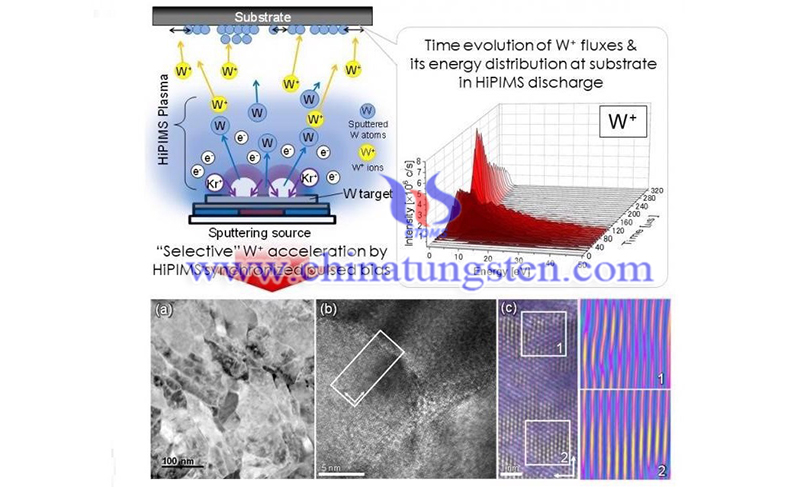
At Tokyo Metropolitan University, scientists use high-power impulse magnetron scattering (HiPIMS) sputtering technology to create tungsten films with unparalleled low film stress levels.
The researchers improved the timing of the "substrate bias pulse" with microsecond precision to reduce impurities and defects to develop a crystalline film with stress as low as 0.03 GPa, similar to the film achieved by annealing. This research is expected to provide an effective way for the electronics industry to manufacture metal thin films.
Modern electronics are based on the complex nanoscale deposition of thin metal films on the surface. Although this sounds easier, it is not. If improperly implemented, the "film stress" generated from the microscopic internal structure of the film can cause years of bending and buckling. Generally, heating or "annealing" is required to eliminate this stress.

Unfortunately, most metals suitable for this work, such as tungsten, exhibit a high melting point, which means that the film must be heated above 1000 °C. In addition to being energy-intensive, this also severely limits the applicable substrates. Therefore, people are vying to use high melting point metals to make thin tungsten films.
Sputtering involves the use of high voltage across the metal "target" and substrate, thereby generating a plasma of charged gas atoms, which bombards the metal target and produces a charged metal vapor. Such metal ions tend to fly to the substrate on which the thin film is formed.
As far as HiPIMS is concerned, the voltage appears in the form of short and strong pulse trains. After each pulse, there is a certain interval between the metal and gas ions reaching the substrate, synchronous "substrate bias" pulses can help selectively accelerate the metal ions, resulting in a denser film. However, despite the many measures taken, the problem of residual stress still exists.
Currently, with the help of tungsten and argon targets, researchers have studied in unparalleled detail how ions with various energies reach the substrate over time. Instead of using a bias pulse triggered at the same time as the HiPIMS pulse, they used their expertise in when the various ions arrived and added a small delay of 60 μs to accurately select when the high-energy metal ions arrived.
The researchers found that sputtering technology helps reduce the amount of gas that eventually enters the film and effectively transfers high levels of kinetic energy. The result is a dense crystalline film with low film stress and large grains.
Making the bias stronger helps the films become highly stress-free. In fact, the effective transfer of energy to the film means that when the film is deposited by them, they have achieved an effect similar to annealing.
In addition, replacing argon with krypton allowed the researchers to produce tungsten films with stress as low as 0.03 GPa, which is equivalent to the stress produced by post-annealing.
An effective way to obtain a stress-free film will have a considerable impact on the metallization process and the production of next-generation circuits. The sputtering technology may be used in other metals and has the potential to bring huge benefits to the electronics industry.
- Next >
Link to this article:Improved Sputtering Technology to Reduce Stress in Tungsten Films
Reprint Statement: If there are no special instructions, all articles on this site are original. Please indicate the source for reprinting:Tungusten,Thanks!^^

