Wafer-Level MoS2 for Integrated Storage and Computing
- Details
- Category: tungsten‘s News
- Published on Tuesday, 29 June 2021 13:06
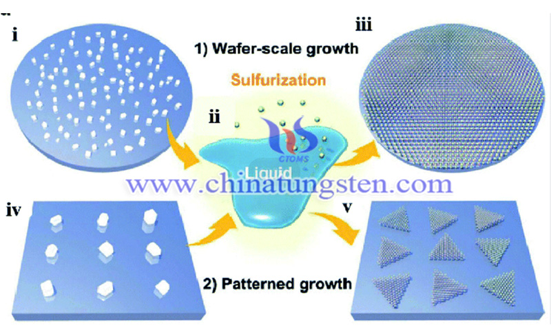
Recently, researchers from the School of Microelectronics of Fudan University have developed a new type of in-memory computing architecture that can be used for multiply-accumulate operations using wafer-level two-dimensional MoS2 semiconductor materials. It has good device durability and can also erase and write operations. It is simple and can realize a long-term multi-value storage capacity to realize analog multiplication and addition operations, thus demonstrating the potential for future low-power and high-calculating integrated storage-calculation applications.

With the continuous development of artificial intelligence, stronger calculating power is required to process a large number of continuous matrix operations, and matrix operations mainly include multiplication and accumulation operations. In the traditional von Neumann computing architecture, the storage and logic operation circuits are separated, and the calculated data needs to be transmitted back and forth between the memory unit and the arithmetic unit, and the bandwidth speed of data transmission has become a further increase in its calculating power.
In addition, although most non-volatile memories can achieve multi-value storing, random errors will cause their recognition accuracy in neural network applications to decrease.

In order to solve the above-mentioned problems, researchers at Fudan University proposed a novel 2T-1C memory computing structure consisting of two MoS2 transistors and a capacitor. The structure is made by using traditional top gate integrated circuit technology, and can realize quick and easy writing of programming information and unlimited flashing and programming operations by using storage cells similar to dynamic random access memory.
In addition, the in-memory calculation structure can also implement hardware-level weight update, in-situ training and self-learning, which can effectively avoid the influence of the device itself on the neural network, so it is necessary for the neural network that requires a huge amount of weight update and learning. There are obvious advantages in training, thus showing its great potential in the future low-power high-computing storage-computing fusion system.

This work was supported by the ASIC National Key Laboratory of Application Specific Integrated Circuits, Fudan University. The research results have been published on Nature Communication as "An In-Memory Computing Architecture Based on Two-Dimensional Semiconductors for Multiply-Accumulate Operations".
- < Prev
- Next >
Link to this article:Wafer-Level MoS2 for Integrated Storage and Computing
Reprint Statement: If there are no special instructions, all articles on this site are original. Please indicate the source for reprinting:Tungusten,Thanks!^^

