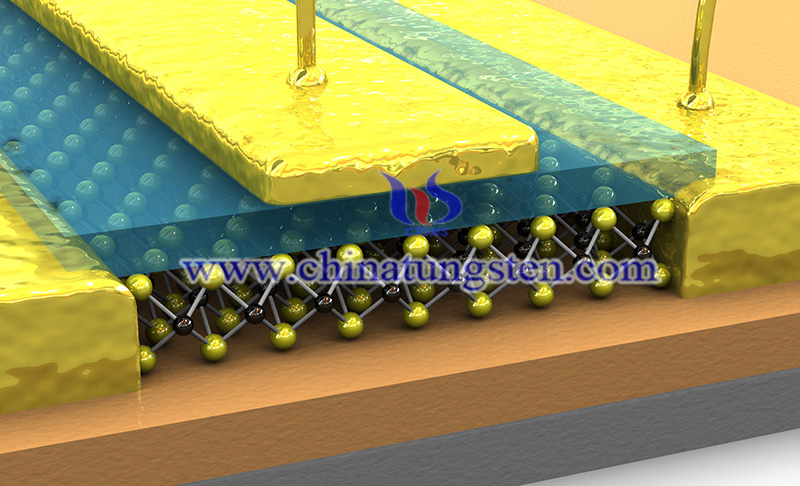
Hunan University Develops 3nm Thick MoS2 Transistor
- Details
- Category: tungsten‘s News
- Published on Thursday, 24 June 2021 21:34
Researchers at Hunan University progress MoS2 transistor as thin as 3 nanometers, with a channel length of only a layer of atoms. The team successfully implemented an ultra-short channel vertical field effect transistor (VFET). The channel length can be shortened to 0.65nm, closely to atom size. The paper of this research was published in Nature Electronics.
It is very harsh to reduce the channel length under 10nm due to the limitations of 他the short channel effect, traditional high-energy metal deposition technology, high-precision photolithography technology, etc. This research provides new ideas for chip performance improvement. First of all, it must be started with the name of metal–oxide–semiconductor field-effect transistor (MOSFET).
"N-type" and "P-type" are two types of semiconductors divided according to polarity, and they can conduct unidirectional conduction. As for the NPN type MOS tube, due to unidirectional conductivity, there are two PN junctions between the NPNs, so they cannot be turned on.

Therefore, an insulating layer of silicon dioxide and a metal plate needs to be placed on top of the P area in turn. This is the gate (G), and the two N-type semiconductors correspond to the drain (D) and the source (S) respectively. After the gate is electrified, it can attract the electrons in the P block between the two N-type semiconductors, thereby forming a channel between the source and drain.
Under the condition of constant width, the shorter the channel length (L), the faster the switching speed. Currently, this value could reach 0.65nm, which is undoubtedly a breakthrough.
Simply put, the researchers used the van der Waals (vdW) metal electrode integration method, using MoS2 as a thin layer or even a single atomic layer of the semiconductor channel. Then, the pre-prepared physical layer of the metal electrode is pressed to the top of the MoS2 channel, and finally, a MoS2 transistor is obtained.
Compared with the traditional metal deposition technology, this new method developed by Hunan University retains the lattice structure and inherent characteristics of the 2D semiconductor, thereby forming an atomic-level flat metal-semiconductor interface and reducing tunneling current.
As the physical limit approaches, chip performance can no longer rely solely on the number of transistors, leading the semiconductor industry is gradually entering the “post-Moore era”.
After testing, the researchers found that when the channel length VFET reaches 0.65nm and 3.6nm, the switching ratios of 26 and 1000 can still be achieved, and the switching ratio performance is improved by two orders of magnitude.
Although the ultra-short channel reduces the switching ratio, low-temperature electrical tests show that this transistor still maintains the characteristic of electron emission.
Besides, this method is universal. The researchers applied this method to layered semiconductors such as tungsten diselenide and tungsten disulfide, and achieved vertical field-effect transistors with a thickness of less than 3nm.
Based on this research of Hunan University, it is expected to further reduce the real physical channel length and get rid of the limitations of high-precision photolithography and etching technology. Not only does it bring hope to the production of sub-3nm MoS2 transistor, it can also be used to improve the process level of van der Waals heterojunction device interfaces.
- < Prev
- Next >
Link to this article:Hunan University Develops 3nm Thick MoS2 Transistor
Reprint Statement: If there are no special instructions, all articles on this site are original. Please indicate the source for reprinting:Tungusten,Thanks!^^

