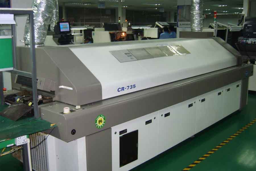
Reflow soldering is to remelt the solder paste pre-distributed on the printed board pads to realize the mechanical and electrical connection between the solder ends or pins of the surface mount components and the printed board pads. Reflow soldering is to solder the components to the PCB board, and reflow soldering is to mount the components on the surface. Reflow soldering relies on the effect of hot airflow on the solder joints. The colloidal flux physically reacts under a certain high temperature airflow to achieve SMD soldering; the reason why it is called “reflow soldering” is because the gas circulates in the soldering machine to generate high temperature to achieve soldering. Purpose.
1. Introduction to the principle and process of reflow soldering
- A. When the PCB enters the heating zone, the solvent and gas in the solder paste evaporate, and at the same time, the flux in the solder paste wets the pads, component ends and pins, and the solder paste softens, collapses, and covers the solder The pad, isolate the pads and component pins from oxygen.
- B. When the PCB enters the heat preservation area, make the PCB and components fully preheated to prevent the PCB from suddenly entering the welding high temperature area and damaging the PCB and components.
- C. When the PCB enters the soldering area, the temperature rises rapidly so that the solder paste reaches a molten state, and the liquid solder wets, diffuses, diffuses, or reflows to the PCB pads, component ends and pins to form solder joints.
- D. The PCB enters the cooling zone, so that the solder joints are solidified and the reflow soldering is completed.
Reflow soldering is an automated soldering process in the SMT production process of electronic products. Reflow soldering is also called reflow soldering, which relies on the continuous reflow of the heat in the furnace, so that the solder paste is dissolved into tin liquid to solder the smt chip components and the circuit board. So it is called reflow soldering because its working principle is to solder the components and the circuit board together by the reflow of hot air in the furnace and the reflow of liquid tin.
2. Introduction to reflow soldering process
The reflow soldering process is a surface-mounted board, and its process is more complicated, which can be divided into two types: single-sided mounting and double-sided mounting.
- A, single-sided mounting: pre-coated solder paste → patch (divided into manual placement and machine automatic placement) → reflow soldering → inspection and electrical test.
- B, double-sided placement: A side pre-coated solder paste → patch (divided into manual placement and machine automatic placement) → reflow soldering → B side pre-coated solder paste → placement (divided into manual placement and machine automatic placement) Mounting) → reflow soldering → inspection and electrical test.
The simplest process of reflow soldering is “screen printing solder paste-patch-reflow soldering. Its core is the accuracy of the screen printing. For the patch, the yield rate is determined by the machine’s PPM. The reflow soldering is to control the temperature rise and the highest Temperature and falling temperature curve.
3. Reflow soldering process requirements
Reflow soldering technology is not unfamiliar in the field of electronic manufacturing. The components on the various boards used in our computers are soldered to the circuit board through this process. The advantage of this process is that the temperature is easy to control, oxidation can be avoided during the welding process, and the manufacturing cost is easier to control. There is a heating circuit inside this device, which heats the nitrogen gas to a high enough temperature and blows it to the circuit board where the component is already attached, so that the solder on both sides of the component is melted and then bonded to the motherboard.
- 1. It is necessary to set a reasonable reflow soldering temperature curve and perform real-time testing of the temperature curve regularly.
- 2. The welding should be carried out in accordance with the welding direction of the PCB design.
- 3. Strictly prevent the vibration of the conveyor belt during the welding process.
- 4. The welding effect of the first printed board must be checked.
- 5. Whether the welding is sufficient, whether the surface of the solder joint is smooth, whether the solder joint shape is half-moon shape, the condition of tin balls and residue, the condition of continuous soldering and virtual soldering. Also check for changes in the color of the PCB surface, etc. And adjust the temperature curve according to the inspection results. The welding quality should be checked regularly during the whole batch production process.
4. Common quality defects and solutions for reflow soldering
The quality of reflow soldering is affected by many factors. The most important factor is the temperature profile of the reflow oven and the number of solder paste components in the electronic production process. Nowadays, the commonly used high-performance reflow soldering furnace can accurately control and adjust the temperature curve more conveniently. In contrast, in the trend of high density and miniaturization, the printing of solder paste has become the key to the quality of reflow soldering. The three factors of paste, stencil and printing can affect the quality of solder paste printing.
Tombstone Phenomenon
In reflow soldering, chip components often stand up, which is called tombstone, also known as suspension bridge and Manhattan phenomenon. This is a defect that often occurs in the reflow soldering process.
Cause: The root cause of the tombstone phenomenon is that the wetting forces on both sides of the components are unbalanced, so the torque at both ends of the components is not balanced, which leads to the tombstone phenomenon.
The following situations will cause the wetting force of both sides of the components to be unbalanced during reflow soldering.
1. The pad design and layout are unreasonable.
If the pad design and layout have the following defects, it will cause the wetting force on both sides of the component to be unbalanced.
One of the pads on both sides of the component is connected to the ground or the area of one side of the pad is too large, and the heat capacity at both ends of the pad is uneven
The temperature difference across the PCB surface is too large to cause uneven heat absorption on both sides of the component pad;
Large-scale devices QFP, BGA, and small chip component pads around the radiator will have uneven temperature at both ends.
Solution: Improve pad design and layout
2. Solder paste and solder paste printing.
The activity of the solder paste is not high or the solderability of the components is poor. After the solder paste is melted, the surface tension is different, which will also cause the pad wetting force to be unbalanced. The amount of solder paste printed on the two pads is uneven, and the more side will absorb more heat due to the solder paste, and the melting time will lag, resulting in unbalanced wetting force.
Solution: Choose a solder paste with higher activity to improve the solder paste printing parameters, especially the window size of the template.
3. Patch.
The uneven force in the Z-axis direction will cause the components to be immersed in the solder paste unevenly, and the wetting force on both sides will be unbalanced due to the time difference during melting. The deviation of the components from the pads will directly lead to tombstones.
Solution: Adjust the process parameters of the placement machine.
4. Furnace temperature curve.
The working curve of PCB heating is not correct, so that the temperature difference on the board surface is too large. Usually, these defects will appear if the reflow furnace body is too short and the temperature zone is too small.
Solution: Adjust the appropriate temperature curve according to each product.
5. Oxygen concentration in N2 reflow soldering.
The use of N2 protective reflow soldering will increase the wetting power of the solder, but more and more reports indicate that the phenomenon of tombstones will increase when the oxygen content is too low; it is generally believed that the oxygen content is controlled at (100-500)× About 10-6mg/m3 is the most suitable.
Tin beads
Tin bead is one of the common defects of reflow soldering, and its reasons are various, not only affecting the appearance but also causing bridging.
Tin beads can be divided into two types. One type appears on one side of the chip component, often in the shape of an independent large ball; the other type appears around the IC pins and is in the shape of scattered small beads.
1. The temperature curve is incorrect.
The reflow curve can be divided into four sections, namely preheating, heat preservation, reflow and cooling. The purpose of preheating and heat preservation is to increase the surface temperature of the PCB to 150°C within 60-90s and keep it warm for about 90s. This can not only reduce the thermal shock of PCB and components, but also ensure the solvent energy part of the solder paste. Volatile, to avoid splashing caused by too much solvent during reflow soldering, causing the solder paste to rush out of the pad and form tin beads.
Solution: Pay attention to the heating rate, and take a moderate preheating so that there is a good platform to make most of the solvent volatilize.
2. The quality of solder paste.
The metal content in the solder paste is usually (90±0.5)%. Too low metal content will lead to too much flux. Therefore, too much flux will cause flying beads due to the fact that it is not easy to volatilize during the preheating stage.
Increased water vapor and oxygen content in solder paste can also cause flying beads. Since solder paste is usually refrigerated, when it is taken out of the refrigerator, there is no guarantee of recovery time, so water vapor will enter; in addition, the lid of the solder paste bottle must be tightly closed after each use. If it is not tightly closed in time, it will also cause Entry of water vapor.
After the solder paste printed on the template is completed, the remaining part should be treated separately. If it is put back in the original bottle, the solder paste in the bottle will deteriorate and tin beads will also be produced.
Solution: Choose high-quality solder paste and pay attention to the storage and use requirements of solder paste.
3. Printing and patching
In the solder paste printing process, due to the offset between the template and the pad, if the offset is too large, the solder dipping will flow out of the pad, and solder balls are likely to appear after heating. In addition, the poor printing environment can also lead to the formation of tin beads. The ideal printing environment temperature is (25±3) ℃, and the relative humidity is 50%~65%.
Solution: carefully adjust the clamping of the template to prevent loosening; improve the printing working environment.
The Z-axis pressure during the placement process is also an important cause of tin beading, which is often not easy to attract people’s attention. The Z-axis head of some placement machines is positioned according to the thickness of the components. If the height of the Z-axis is adjusted incorrectly, it will It causes the phenomenon that the solder paste is squeezed out of the pad when the components are attached to the PCB. This part of the solder paste will form tin beads during soldering. The tin beads produced in this case are slightly larger in size.
Solution: readjust the height of the Z axis of the placement machine.
The thickness of the template and the size of the opening. If the template thickness and opening size are too large, the amount of solder paste will increase, and it will also cause the solder paste to overflow to the outside of the pad, especially the template manufactured by chemical etching.
Solution: Choose a template with an appropriate thickness and the design of the opening size. Generally, the opening area of the template is 90% of the pad size, which will improve the solder ball situation.
4. Wicking phenomenon
The wicking phenomenon, also known as the core-pulling phenomenon, is one of the common soldering defects, which is more common in vapor reflow soldering. Wicking is the phenomenon that the solder detaches from the pad and travels along the lead to between the lead and the chip body, which usually results in a serious virtual soldering phenomenon.
Cause: The main reason is that the thermal conductivity of the component pins is large, so the temperature rises rapidly, so that the solder preferentially wets the pins, and the wetting force between the solder and the pin is much greater than the wetting force between the solder and the pad. , The upturn of the lead will aggravate the occurrence of wicking phenomenon.
Solution:
For vapor-phase reflow soldering, the SMA should be fully preheated first and then put into the vapor-phase furnace;
The solderability of PCB pads should be carefully checked. PCBs with poor solderability should not be used in production;
Full attention is paid to the coplanarity of components, and devices with poor coplanarity should not be used in production.
In infrared reflow soldering, the organic flux in the PCB substrate and the solder is a good infrared absorbing medium, while the pins can partially reflect the infrared. Therefore, the solder is preferentially melted, and the wetting power of the solder and the pad is limited. Will be greater than the wetting force between the solder and the lead, so the solder will not rise along the lead, so the probability of wicking phenomenon is much smaller.
5. Bridging
Bridging is one of the common defects in SMT production. It will cause short circuits between components and must be repaired when the bridging is encountered.
There are many reasons for bridging, and there are four common ones:
The quality of solder paste.
The metal content in the solder paste is too high, especially after the printing time is too long, the metal content is likely to increase, leading to IC pin bridging;
The solder paste has low viscosity and flows out of the pad after preheating;
The solder paste has a poor slump and flows out of the pad after preheating.
Solution: Adjust the solder paste ratio or use good quality solder paste.
Printing system.
The printing machine has poor repeat accuracy and misalignment (the steel plate is not well aligned, the PCB is not well aligned), which causes the solder paste to be printed outside the pad, which is mostly seen in the production of fine-pitch QFP;
The design of the window size and thickness of the steel plate is incorrect, and the Sn-Pb alloy coating of the PCB pad design is uneven, resulting in a large amount of solder paste.
Solution: Adjust the printer to improve the coating layer of the PCB pad.
Post and place.
Excessive placement pressure and flooding of solder paste after pressure are common reasons in production. In addition, the placement accuracy is not enough, the components are shifted, and the IC pins are deformed. It is also easy to cause bridging.
Preheat.
The heating rate of the reflow oven is too fast, and the solvent in the solder paste is too late to volatilize.
Solution: Adjust the height of the Z axis of the placement machine and the heating rate of the reflow oven.
Link to this article: What Is Reflow Soldering
Reprint Statement: If there are no special instructions, all articles on this site are original. Please indicate the source for reprinting:https://www.cncmachiningptj.com/,thanks!
 PTJ® provides a full range of Custom Precision cnc machining china services.ISO 9001:2015 &AS-9100 certified. 3, 4 and 5-axis rapid precision CNC machining services including milling, sheet metal to customer specifications,Capable of metal & plastic machined parts with +/-0.005 mm tolerance.Secondary services include CNC and conventional grinding, laser cutting,drilling,die casting,sheet metal and stamping.Providing prototypes, full production runs, technical support and full inspection.Serves the automotive, aerospace, mold&fixture,led lighting,medical,bicycle, and consumer electronics industries. On-time delivery.Tell us a little about your project’s budget and expected delivery time. We will strategize with you to provide the most cost-effective services to help you reach your target,Welcome to Contact us ( [email protected] ) directly for your new project.
Link to this article:What Is Reflow Soldering?
Reprint Statement: If there are no special instructions, all articles on this site are original. Please indicate the source for reprinting:Tungusten,Thanks!^^

